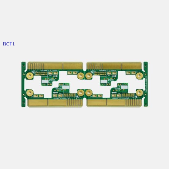
UL&IPC Standard &ISO
Layer: 2L
Material: Fr-4
PCB Thickness: 1.2mm
Cu Thickness: 2.0 OZ
Min Line W/S: 0.1/0.1mm
Surface Finish: Immersion gold
Certificate: UL/ISO/TS16949
Application: Industrial Control
Item | Speci. |
Layers | 1~32 |
Board thickness | 0.1mm-7.0mm |
Material | FR-4,CEM-1/CEM-3,PI,High Tg,Rogers |
Max panel size | 32"×48"(800mm×1200mm) |
Min hole size | 0.075mm |
Min line width | 3mil(0.075mm) |
Surface finish | OSP,HASL,Imm Gold/Nickel/Ag, Electric gold |
Copper thickness | 0.5-7.0OZ |
Soldermask | Green/Yellow/Black/White/Red/Blue |
Silkscreen | Red/Yellow/Black/White |
Min PAD | 5mil(0.13mm) |
Inter package | Vacuum |
Outer package | Carton |
Outline tolerance | ±0.75mm |
Hole tolerance | PTH:±0.05 NPTH:±0.025 |
Certificate | UL,ISO 9001,ISO14001,IATF16949 |
Special request | Blind hole+Gold finger + BGA |
Material Suppilers | Shengyi, KB, Nanya, ITEQ,etc. |
The double-sided PCB is a common type of printed circuit board. It has wires and components on both the front and back sides, and the double-sided PCB boards are connected with vias in the middle. The double-sided printed circuit board has two upper and lower conductor patterns, and the upper and lower via holes are connected by expensive perforations. In the processing of printed circuit boards, the hole walls of your perforated holes are coated with a copper layer to make the upper and lower layers conductive. Double-sided printed circuit boards are usually double-sided copper-clad laminates, using screen printing or photo imaging. A resist pattern is formed on the copper surface, and excess copper foil is removed by chemical etching to form a conductor pattern.
Prepare the circuit schematic
Create a new PCB file and load it into the component package library
Planning the circuit board
Load the netlist and components
Automatic layout of components
Layout adjustment
Network density analysis
Wiring rule setting
Automatic wiring
Manually adjust the wiring
After the components of the double-layer PCB are drawn in the EDA software, the wiring sequence is first designed as power line, sensitive line, high frequency line and low frequency line. It is best to have a separate power supply for the key lead, a ground return, and the lead is very short, so sometimes a ground wire is placed close to the signal line on the edge of the key lead to make it form the smallest working loop.
The signal lines of the double-layer PCB board are the key crystal, crystal oscillator circuit, clock circuit, CPU and other signal lines, which must comply with the principle that the circulating area is as small as possible.
PCB Prototype | Quick Turn PCB | Single-Sided PCB |
Double-Sided PCB | Multilayer PCB | Rigid PCB |
Flexible PCB | Rigid-Flex PCB | LED PCB |
Aluminum PCB | Metal Core PCB | Thick Copper PCB |
HDI PCB | BGA PCB | High TG PCB |
PCB Stencil | Impedance Control PCB | PCB Assembly |
High-Frequency PCB | Bluetooth Circuit Board | Automotive PCB |
USB Circuit Board | Halogen-Free PCB | Antenna PCB |
SEND MESSAGE
If you are interested in our products and want to know more details,please leave a message here,we will reply
CONTACT US
E-main:admin@bdctl.com
803, Building 38, Tangshuiwei Old Village, Minzhi Street, Longhua District, Shenzhen
PCB Factory: No. 2F to 6F, NO.1 Xingye Road, Xiaolan Town, Zhongshan City, Guangdong Province
The first floor of the above address is SMT processing plant